What is a transistor?
A transistor is a miniature semiconductor that regulates or controls current or voltage flow in addition to amplifying and generating these electrical signals and acting as a switch or gate for them. Typically, transistors consist of three layers, or terminals, of a semiconductor material, each of which can carry a current.
Transistors are crucial components of modern electronics. When working as an amplifier, a transistor transforms a small input current into a bigger output current. As a switch, it can be in one of two distinct states -- on or off -- to control the flow of electronic signals through an electrical circuit or electronic device.
Why transistors are important
A transistor has only one circuit element. In small quantities, transistors are used to create simple electronic switches. They're the basic elements in integrated circuits (ICs), which consist of a large number of transistors interconnected with circuitry and baked into a single silicon microchip.
In large numbers, transistors are used to create microprocessors where millions of transistors are embedded into a single IC. They also drive computer memory chips and memory storage devices for MP3 players, smartphones, cameras and electronic games. Transistors are embedded in nearly all ICs, which are part of every electronic device.
Transistors are also used for low-frequency, high-power applications, such as power-supply inverters that convert alternating current into direct current. Additionally, high-frequency applications use transistors, such as the oscillator circuits that generate radio signals.

How transistors revolutionized the tech world
Transistors were invented at Bell Laboratories in 1947. These solid-state devices rapidly replaced the bulky vacuum tube as an electronic signal regulator. The invention of the transistor fueled the trend to miniaturize electronics. They're now considered one of the most significant developments in the history of the PC.
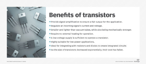
Transistors are smaller, lighter and consume less power than vacuum tubes. As a result, electronic systems made with them are also smaller, lighter, faster and more efficient than ones made with vacuum tubes. Transistors are also stronger, require less power and, unlike vacuum tubes, don't require external heaters.
As the size of transistors decreased, their costs fell, creating more opportunities to use them. Integrating transistors with resistors and other diodes and electronics components makes ICs smaller. This miniaturization relates to Moore's Law, which states that the number of transistors in a small IC would double every two years.

Transistors explained
A semiconductor device, which conducts electricity in a semi-enthusiastic way, falls somewhere between a real conductor like copper and an insulator such as the plastic wrapped around wires. Although most transistors are made from silicon, they also use other materials such as germanium and gallium arsenide.
Silicon, a chemical element often found in sand, isn't normally a conductor of electricity. A chemical process called doping introduces impurities into a semiconductor to modulate electrical, optical and structural properties. This enables silicon to gain free electrons that carry electric current. The silicon becomes either an n-type semiconductor where electrons flow out of it or a p-type semiconductor where electrons flow into it. Either way, the semiconductor enables the transistor to function as a switch or amplifier.
A transistor's three-layer structure contains one of the following layers:
- An n-type semiconductor layer between two p-type layers in a positive-negative-positive (PNP) configuration.
- A p-type layer between two n-type layers in a negative-positive-negative (NPN) configuration.
Regardless of its configuration, the inner semiconductor layer acts as the control electrode, or conductor, letting electricity enter or leave. A small change in the current or voltage at this layer produces a large, rapid change in the current passing through the entire component, enabling the transistor to function. This change occurs at the junction of both the n-type and p-type layers, also called the depletion region, which acts as an insulator.

How transistors work
A transistor operates as a switch or gate for electronic signals, opening and closing an electronic gate many times per second. It ensures the electronic circuit is on if the current is flowing and switched off if it isn't. Complex switching circuits that make up all modern networking and telecommunications systems rely on transistors. Circuits also offer high switching speeds, such as hundreds of gigahertz or more than 100 billion on-and-off cycles per second.
Transistors are combined to form a logic gate, which compares multiple input signals to provide a different output. Computers with logic gates can make simple decisions using Boolean algebra. These techniques are the foundation of modern-day computing and computer programs.
Transistors also play an important role in amplifying electronic signals. For example, in radio applications such as FM receivers, where the received electrical signal is weak due to disturbances, amplification provides audible output. Transistors increase signal strength to provide this amplification.
Parts of a transistor
A transistor is similar to a set of two diodes with their cathodes or anodes tied together. It has three terminals that carry electrical current and help make a connection to external circuits:
- The emitter is the transistor's negative lead.
- The base is the terminal that activates the transistor.
- The collector is the transistor's positive lead.
NPN transistors have a p-type silicon base. It's sandwiched between two layers of n-type silicon -- the emitter and collector.
The emitter is moderately sized and heavily doped. Its primary function is to supply the electrons, known as the majority carriers, that carry most of the electrical current. It's called the emitter because it emits electrons.
The base is the center terminal between the emitter and the collector. It's thin and lightly doped. Its main purpose is to pass the carriers from the emitter to the collector.
The collector collects carriers sent by the emitter via the base. It's moderately doped and larger than both the emitter and base.
The emitter, base and collector have the same functions in a PNP circuit. The only difference in the PNP transistor is that the n-type base is layered between the p-type emitter and collector. The NPN versus PNP configurations determine the direction of the emitter's arrow, which is always part of the emitter-base junction. The arrow points out for an NPN circuit and in for a PNP circuit.
Types of transistors
There are two major types of transistors:
- Bipolar junction transistor (BJT).
- Field-effect transistor (FET).
A BJT is one of the most common types of transistors and can be either NPN or PNP. This means a BJT consists of three terminals: the emitter, the base and the collector. By joining these three layers, a BJT can amplify an electrical signal and switch the current on and off.
Two kinds of electrical charge -- electrons and holes -- create the amount of current flow. The BJT's base-emitter junction is forward-biased with a small emitter resistance, while the base-collector junction is reverse-biased with a large resistance.
In a PNP-type BJT, conduction happens through holes or the absence of electrons. The collector current is slightly less than the emitter current. Changes in the latter affect the former. The base controls the base current flow from the emitter to the collector. In this case, the emitter emits holes, which the collector then collects.
In an NPN-type BJT, electrons pass from the emitter to the base and are collected by the collector. When this happens, conventional current flows from the collector to the emitter. The base controls the number of electrons the emitter emits.
In both NPN and PNP-type BJTs, amplification is possible when they operate in active region or active mode where the base controls the flow of current between the emitter and collector. As the base current increases, the output current also increases and amplifies.
An FET also has three terminals -- source, drain and gate -- which are analogous to a BJT's emitter, collector and base, respectively. In the FET, the n-type and p-type silicon layers are arranged differently from those of the BJT. They are also coated with layers of metal and oxide to create the metal-oxide semiconductor field effect transistor (MOSFET).
In the FET, field effect refers to an effect that enables the flow of current and switches the transistor on. Electrons can't flow from the n-type source to the drain because the p-type gate between them contains holes. But attaching a positive voltage to the gate creates an electric field that enables electrons to flow from the source to the drain. This creates the field effect, which facilitates the flow of current in the FET.
FETs are commonly used in low-noise amplifiers, buffer amplifiers and analog switches. The metal-semiconductor field-effect transistor is often used for high-frequency applications, such as microwave circuits.
Other transistor types include the following:
- Junction field effect transistor, a three-terminal semiconductor essential in precision-level, voltage-operated controls in analog electronics.
- Thin-film transistor, a type of FET often used in liquid crystal displays.
- Schottky transistor, which combines a transistor and a Schottky diode known for extremely fast switching to keep the transistor from saturating by diverting excessive input current.
- Diffusion transistor, which is a type of BJT formed by the diffusion of dopants onto a substrate.
How are transistors used in power electronics?
Power electronics, such as power supply units or audio amplifiers, require transistors. Their ability to switch high amounts of power on and off quickly lets them control the flow of electrical power in these devices while minimizing risks. Transistors are also useful in high-power, large-scale equipment and systems, such as electric vehicles, wind turbines, solar panels and other renewable energy-generating devices.
BJTs and MOSFETs are the types of transistors used in power electronics, along with insulated-gate bipolar transistors. IGBTs combine the strengths of BJTs and MOSFETs; they handle current the way BJT does but have the voltage control of a MOSFET. This makes them viable alternatives to BJTs and MOSFETs.
How does the size of a transistor affect performance?
Over time, as transistors have advanced, they have also become smaller in size, which improves their performance. There are a few reasons why the consensus among industry experts is that smaller transistors mean improved performance. They include the following:
- More space inside chips. When transistors are smaller, they create more space inside the microchips housing them for more transistors and combinations to fit. This enhances computational power.
- Faster current switching. Smaller transistors mean less distance for electrons to travel. Shorter distances to travel mean faster current switching times.
- Lower power consumption. Small transistors require smaller voltages while larger ones require higher voltage.
- Improved processing speed. The increased number of transistors inside a chip combined with faster current switching leads to improved processing speeds.
The future of transistors
Newer innovations in transistors point the way to future developments. Smaller size and increased efficiency are certainly the road to the future, as exemplified by new transistor designs. These include forksheet transistors and nanosheet structures, which are more compact and faster than current designs. Companies such as IBM are researching and testing new nanosheet innovations.
There is often talk of quantum computing and how quantum computers will perform certain processing tasks faster than traditional computers relying on transistors. However, the idea that quantum computers will replace transistor-based computing on a large scale isn't likely in the foreseeable future. It's more likely that the transistor-based technology will remain important for everyday tasks while companies building quantum computers could apply them to more complex processing tasks, such as analyzing massive data sets that are too compute-intensive for traditional computers.
Central processing units (CPUs) and microprocessors both use transistors. That's one way they're similar. Learn about the differences between CPUs and microprocessors.