Fotolia
NAND flash memory basics: Comparing SLC, MLC and TLC NAND
NAND is the most popular type of flash, but there are many different types, and they each serve a different purpose. Do you know your NAND flash basics?
The majority of solid-state drives in enterprise data centers are based on NAND flash memory. But not all NAND storage is the same, particularly when it comes to performance, endurance and cost. Companies considering a NAND purchase need to know their NAND flash memory basics.
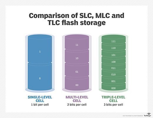
There are several different kinds of NAND, each one slightly different. At the heart of these differences is the number of bits stored in each cell. Today's drives store one, two or three bits per cell. Although supporting technologies also play a role -- as do other architectural features -- the bit number remains one of the primary factors in determining a drive's capabilities, both directly and indirectly.
Get to know NAND flash memory basics
NAND flash is a type of nonvolatile memory, which means it can store a charge whether or not the drive is connected to a power supply. There are other types of flash storage, but NAND is the predominant architecture used in today's SSD storage.
A NAND drive is made up of one or more flash chips. Each chip contains multiple dies, and each die contains multiple planes -- usually two. The planes are divided into blocks, the blocks into pages and the pages into cells, which is where the bits are stored. Although data is read and written at the page level, it can be erased only at the block level. This results in complex write-erase processes.
Learn more about the pricing of different types of flash.
A NAND drive also comes with a controller to manage data operations and address write-erase complexities. The controller is a drive-specific processor that executes the firmware and handles advanced operations such as wear leveling, garbage collection, encryption, bad-block mapping and error code correction (ECC).
Single-level cell NAND flash memory basics
When reading, writing or erasing data, a NAND drive uses the voltage state of the applicable cells to determine or set their bit settings. The most basic NAND chip is limited to only one bit of data per cell. As a result, the cell is always in one of two states: programmed (0) or erased (1). The controller determines the state by the level of voltage applied to the cell.
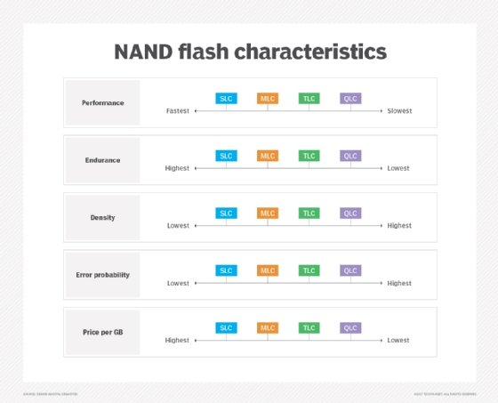
A NAND chip that contains only one bit per cell is referred to as single-level cell (SLC) flash. Because only one bit is stored per cell, the controller can determine the cell's state quickly and easily, without incurring the number of errors generated by multi-bit cell architectures. As a result, the SLC chip performs better and is more reliable than a multi-bit chip.
All flash chips support only a limited number of write-erase operations. For SLC flash, that number is about 100,000 before failure. Chips that contain more than one bit per cell have a much lower threshold because of the additional wear on each cell.
A drive based on SLC flash owes much of its success to the advanced capabilities built into the controller and its firmware, along with caching and over-provisioning. Even so, it is the single-cell architecture that drives the performance and endurance behind SLC flash. Unfortunately, these capabilities also come with a hefty price tag.
Multi-level cell NAND flash memory basics
To bring down costs, vendors produce multi-level cell (MLC) flash, in which two bits of data are stored in each cell, which results in greater capacities at lower prices per bit. Despite the multi part of the name, MLC usually refers to a two-bit structure.
Unfortunately, MLC flash doesn't perform as well as SLC flash. It is also more prone to data corruption and has a much lower level of endurance. For example, because of the higher bit rate per cell, voltage readings must be much more precise, which makes the chip more susceptible to high temperatures. In addition, cell-level operations are more complex because of the need to navigate the extra bit per cell.

The higher rate of data corruption also requires more robust ECC processes, which can affect performance even further. In addition, the physical mechanisms that control the voltage state wear out faster, which results in a write-erase threshold between 3,000 and 10,000 before failure -- much lower than SLC flash.
But, as with SLC flash, MLC flash uses wear leveling, garbage collection, caching, over-provisioning and other advanced techniques to deliver SSDs that maximize reliability and endurance.
In addition, some vendors also offer enterprise MLC (eMLC) flash, which decreases the speed and density of data written to the cell, but still uses the MLC architecture. This approach can extend endurance by three times that of traditional MLC to achieve up to 30,000 write-erase cycles, and it's still a cheaper alternative to SLC flash. That said, eMLC flash does not perform as well as MLC flash.
Triple-level cell NAND flash memory basics
Because of the ever-increasing demands of enterprise data, vendors continue to work to perfect triple-level cell (TLC) flash, which stores three bits of data per cell. As part of these efforts, vendors are trying to squeeze the extra bits into smaller cells so more cells can fit on a chip. The result is a substantial increase in density over SLC and MLC flash. This helps drop SSD prices even further.
The challenge with flash, however, is that, as densities increase, voltage operations become more sensitive and data management more complex. This results in even lower performance, higher error rates and fewer write-erase cycles than MLC flash. In addition, because the cells are closer together, the controller must be even more precise in determining and setting the voltage states of the participating cells. The greater bit rates also cause cell layers to erode even faster.

Because of these limitations, the expected lifespan for TLC flash is only 500 to 1,000 write-erase cycles before the chip fails. Many organizations use TLC flash only for read-heavy workloads rather than write-intensive ones.
As with MLC flash, supporting technologies advance quickly. Before long, TLC flash could support other types of workloads much better. For now, organizations will likely want to stick with SLC or MLC flash for their critical write-intensive applications, unless a newer technology can make TLC flash a more viable alternative, such as 3D NAND.
3D NAND flash memory basics
The typical NAND flash chip contains a single layer of memory cells, referred to as a planer layout. By increasing bit rates and shrinking cell sizes, vendors have been able to produce SSDs with greater densities at lower prices per gigabyte. But these greater densities also result in more electrical interference and lower endurance, which makes it difficult to push beyond the current planar thresholds.
To address NAND's physical limitations, vendors turn to 3D NAND, which stacks memory cells into multiple layers in the silicon to create a vertical layout. Each layer is based on an MLC or TLC architecture, but the cells are spaced out more than in a planar layout. This results in a lower rate of electrical consumption and interference, but still achieves greater densities.
The layered architecture in 3D NAND can help boost reliability, maximize endurance and deliver higher write performance over planar multi-cell flash, and bring down the cost per bit even further. 3D NAND also makes TLC flash a more viable alternative for write-intensive enterprise applications. The newer architecture might even make quad-level cell (QLC) flash a more feasible prospect in the not-too-distant future.
The biggest challenge with 3D NAND is manufacturing the chips, which calls for a high degree of precision to perfectly align the layers and blocks. Vendors must also make a substantial investment in the technology necessary to produce the chips before they can get started. Companies such as Samsung, Intel and Micron lead the way, and 3D NAND is on track to become the definitive standard for enterprise SSDs.


